Ultrathin Solar Cells Reach Nearly 20% Efficiency
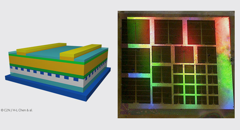
Researchers at the French Centre de Nanosciences et de Nanotechnologies (C2N) have succeeded, in collaboration with researchers at Fraunhofer ISE and others, to efficiently trap sunlight in a solar cell thanks to an ultrathin absorbing layer made of 205 nm-thick gallium arsenide (GaAs) on a nanostructured back mirror. With this new process of fabrication, an efficiency of nearly 20% was obtained.
Up to now, the state-of-the-art 20%-efficient solar cells fabricated from GaAs required at least 1 micrometer-thick layers of semiconductor material, or even 40 µm or more in the case of silicon. Thinning the absorber automatically reduces absorption of sunlight and conversion efficiency. A flat mirror at the backside of the cell can help and lead to double-pass absorption, but no more. Yet, a stronger thickness reduction would enable material savings of scarce materials and industrial throughput improvements due to shorter deposition times. But previous attempts of light trapping have been greatly limited in performance by the optical and electrical losses.
Researchers of the team led by Stéphane Collin at the Centre for Nanoscience and Nanotechnology – C2N (CNRS/Université Paris-Saclay), in collaboration with Fraunhofer ISE in particular, have developed a new strategy to trap light in ultrathin layers made of only 205 nm-thick gallium arsenide, a semiconductor of the III-V family. The guiding idea was to conceive a nanostructured back mirror to create multiple overlapping resonances in the solar cell, identified as Fabry–Perot and guided-mode resonances. They constrain light to stay longer in the absorber, resulting in efficient optical absorption despite the low quantity of material. Thanks to numerous resonances, absorption is enhanced over a large spectral range that fits the solar spectrum from the visible to the infrared. Controlling the fabrication of patterned mirrors at the nanometer scale was a key in the project. The team used nanoimprint lithography to directly emboss a sol-gel derived film of titanium dioxide, an inexpensive, rapid and scalable technique.
“Together with our French partners we are very happy about this result and its publication in the renowned journal “Nature Energy”, says Dr. Frank Dimroth, Head of the Department “III-V Photovoltaics and Concentrator Technology” at Fraunhofer ISE. And he adds: “We expect to be able to even further improve the efficiency of ultrathin solar cells”. The work published in Nature Energy demonstrates that this architecture should enable 25% efficiency in the short term. Even if the limits are still unknown, researchers are convinced that the thickness could be further reduced without efficiency loss, at least by a factor of two. GaAs solar cells are still commercially limited to space application due to their cost. However, researchers are already working to extend this concept for large-scale photovoltaics made of e.g. CdTe, CIGS or silicon materials.