Fraunhofer ISE: Kerfless Wafer Technology to Bring Cost of Photovoltaics Down and Reduce Waste
The global market for photovoltaics (PV) is expected to grow by 25% in 2015, with similar increase in the years to follow.
The price for PV modules has come down drastically, however, there is still great potential for further reduction in the value chain. However, the industry needs disruptive approaches to increase the module efficiency and to reduce the material and energy consumption in production. In this context, the Fraunhofer Institute for Solar Energy Systems ISE announces the start of a new spin off company: NexWafe will transfer Fraunhofer ISE’s kerfless wafer technology into production. Founder and CEO of NexWafe is Stefan Reber, formerly Head of the Department Crystalline Silicon – Materials and Thin Film Solar Cells at Fraunhofer ISE. The start-up is being supported by seed funding from Fraunhofer Venture.
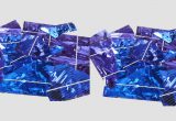
NexWafe’s products will serve the multibillion dollar high-end wafer market with its disruptive kerfless wafer technology. Being based on epitaxy, the kerfless wafer, which has been developed throughout the last fifteen years, is a drop-in replacement for conventional wafers produced by a single-crystal ingot and wire sawing process. NexWafe´s kerfless wafers enable significant cost reduction in solar cell production.
Stefan Reber and his team at Fraunhofer ISE have developed a reliable epitaxial deposition process for crystalline silicon layers, which is transferable to the photovoltaic industry. The process focus is on atmospheric pressure chemical vapor deposition (APCVD) at temperatures up to 1300°C. This process is well-known from microelectronics, but had to be radically adapted for photovoltaic applications in terms of throughput of the equipment. Stefan Reber and his team of 30 people have developed different generations of deposition reactors, ranging from very flexible batch-type laboratory setups to large multi-chamber in-line systems with the option of continuously depositing p- and n-doped epitaxial layers. The latest development, a reactor named ProConCVD, has been designed for high throughput as required in industrial production, demonstrating low-cost high-quality silicon epitaxy for PV.
NexWafe has the unique opportunity to leverage extensive R&D work done as well as the infrastructure of the institute, to take the kerfless wafer technology to mass production. ”I’m excited about the opportunity to transfer this outstanding R&D work, which has been carried out over a long period of time into a commercially successful product that is based on our kerfless wafer technology”, says Andreas Bett, Director of the Division Materials – Solar Cells and Technology as well as Deputy Director of Fraunhofer ISE. His former colleague and now NexWafe CEO Stefan Reber adds: “For me it is a unique and exciting moment to transfer the results of our extensive work into business and help to leverage this exciting technology.” Eicke R. Weber, Fraunhofer ISE Director concludes: “I’m convinced that with this excellent founding team, NexWafe will contribute a big share to further decrease the cost of silicon photovoltaics substantially.”